- Created2024.11.07
Fabrication of 4-Inch Wafer-Scale Heterostructure via PECVD drives AI Semiconductor Performance Innovation!
- KIMM Achieves World’s First Large-Area Semiconductor Fabrication with TMDc and Graphene Heterostructure
- Contribution to Low-Power, High-Performance AI Semiconductor Technology through Plasma Equipment (PECVD)
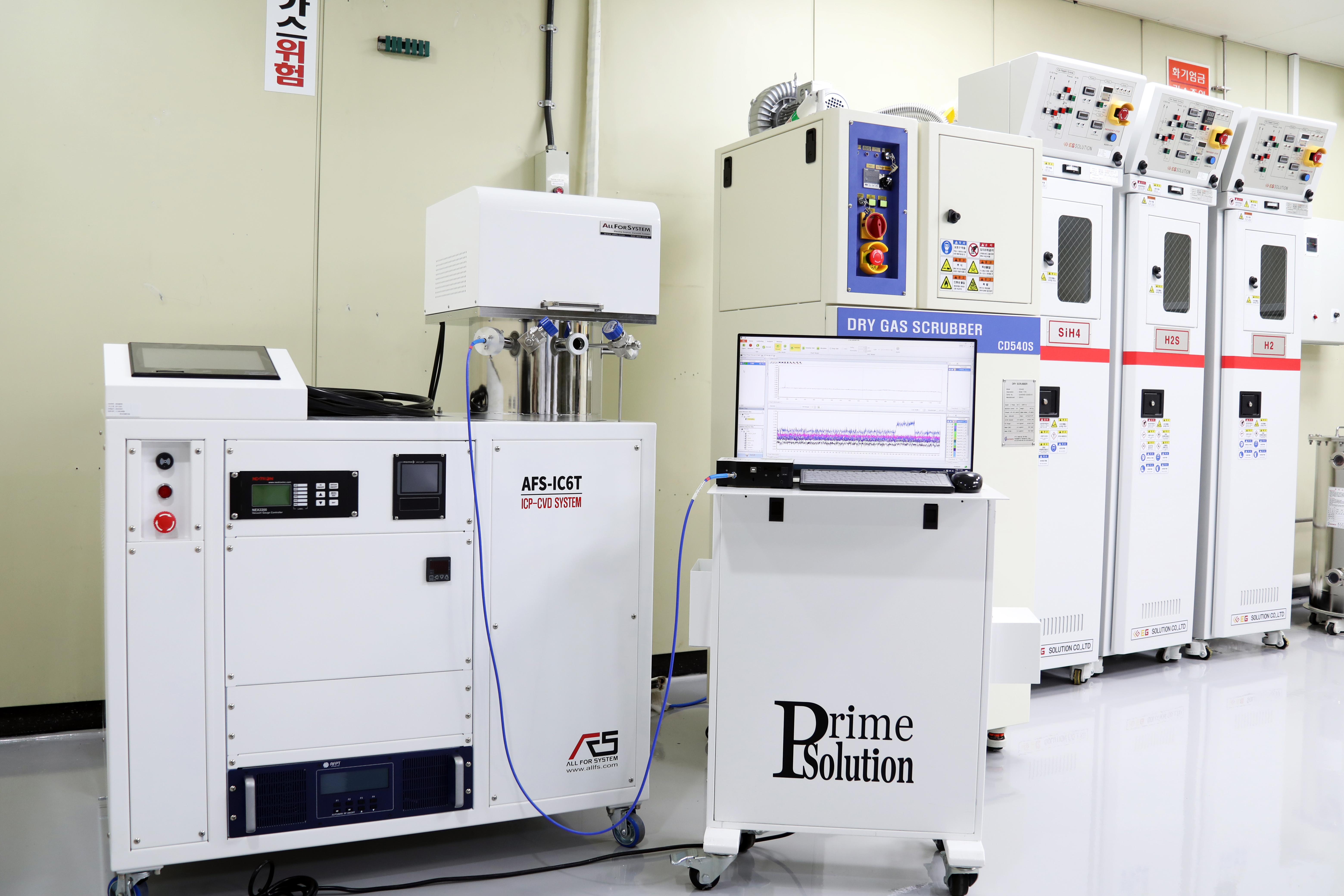
□ As artificial intelligence (AI) technology advances, the demand for higher-performing semiconductors is rapidly growing. The development of new materials and innovative structures to achieve high-performance semiconductors has become crucial. For the first time globally, a 4-inch heterostructure fabrication technology using plasma-enhanced chemical vapor deposition (PECVD) has been developed. This breakthrough enables the production of low-power, high-performance semiconductors, surpassing the capabilities of traditional silicon-based technology.
□ The research team led by Senior Researcher Hyeong-U Kim of the Semiconductor Manufacturing Research Center of the Korea Institute of Machinery and Materials (President Seog-Hyeon Ryu, hereinafter referred to as KIMM), an institute under the jurisdiction of the Ministry of Science and ICT, collaboration with Professor Taesung Kim’s team from the Department of Mechanical Engineering at Sungkyunkwan University (President Yoo Ji-Beom), has achieved the world’s first successful fabrication of a 4-inch heterostructures semiconductor with using plasma technology. This technology is expected to be applicable to AI semiconductors by utilizing next-generation semiconductor materials like TMDc.*
*TMDc (Transition Metal Dichalcogenides): A material candidate for next-generation semiconductors with atomic-level, 2D structures offering silicon-like performance, low power operation, and fast switching speeds. Particularly suitable for neuromorphic systems and used in machine learning, deep learning, and cognitive computing. (e.g., molybdenum disulfide (MoS₂), tungsten disulfide (WS₂), and molybdenum selenide (MoSe₂)).

Senior Researcher Hyeong-U Kim (Co-corresponding Author) from the Semiconductor Manufacturing Research Center at the Korea Institute of Machinery and Materials,
Professor Taesung Kim (Co-corresponding Author) from the Department of Mechanical Engineering at Sungkyunkwan University,
Researcher Hyunho Seok (First Author) from Sungkyunkwan University.
Senior Researcher Hyeong-U Kim(left), from the Semiconductor Manufacturing Research Center
at the Korea Institute of Machinery and Materials' Autonomous Manufacturing Research Division,
is holding a heterostructures semiconductor sample in front of the Plasma synthesis equipment he developed.
□ Using PECVD equipment, the research team succeeded in producing two types of 4-inch wafer-scale heterostructures. The first type, a heterostructure of WS₂ and graphene, was fabricated by depositing a 1-nanometer (nm) tungsten (W) metal layer onto a graphene-transferred wafer, followed by H₂S plasma sulfurization.
□ Additionally, the team achieved a breakthrough with a metal-semiconductor heterostructure by combining two distinct forms of molybdenum disulfide (MoS₂) as thin film. The metallic 1T phase, with an orthorhombic structure, is metastable compared to the more stable hexagonal 2H phase, making large-area wafer production challenging. This new technology allowed the team to produce a 4-inch wafer in the 1T phase and successfully implement the 1T-2H heterostructure.
□ Traditional method for heterostructure, such as stacking, were only allowed to small sizes of a few μm and had reproducibility issues. The team overcame these limitations by using PECVD to fabricate a 4-inch wafer-scale heterostructure. This breakthrough allows for the development of a 3D integrated structure, which significantly reduce power loss and heat dissipation, leading to enhance performance and energy efficiency—key factors for low-power, high-performance AI semiconductors.
□ KIMM’s Senior Researcher Hyeong-U Kim stated, “This newly developed technology not only fulfills wafer-size and reproducibility requirements but also allows experimental validation previously restricted to academic research. Using PECVD, a widely employed tool in the semiconductor industry, this technology offers high potential for mass production, likely contributing to advancements in AI semiconductor performance and commercialization.”
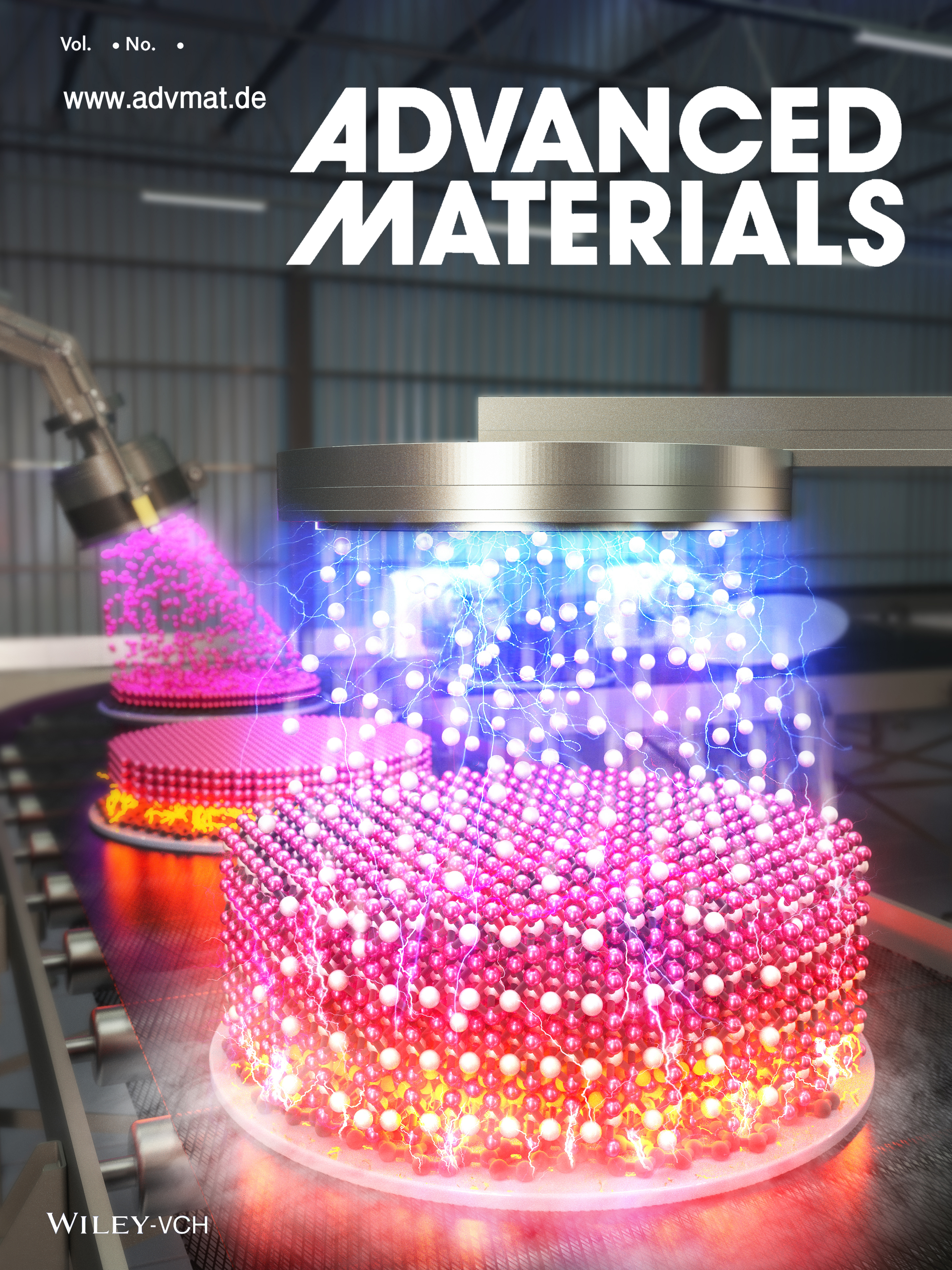
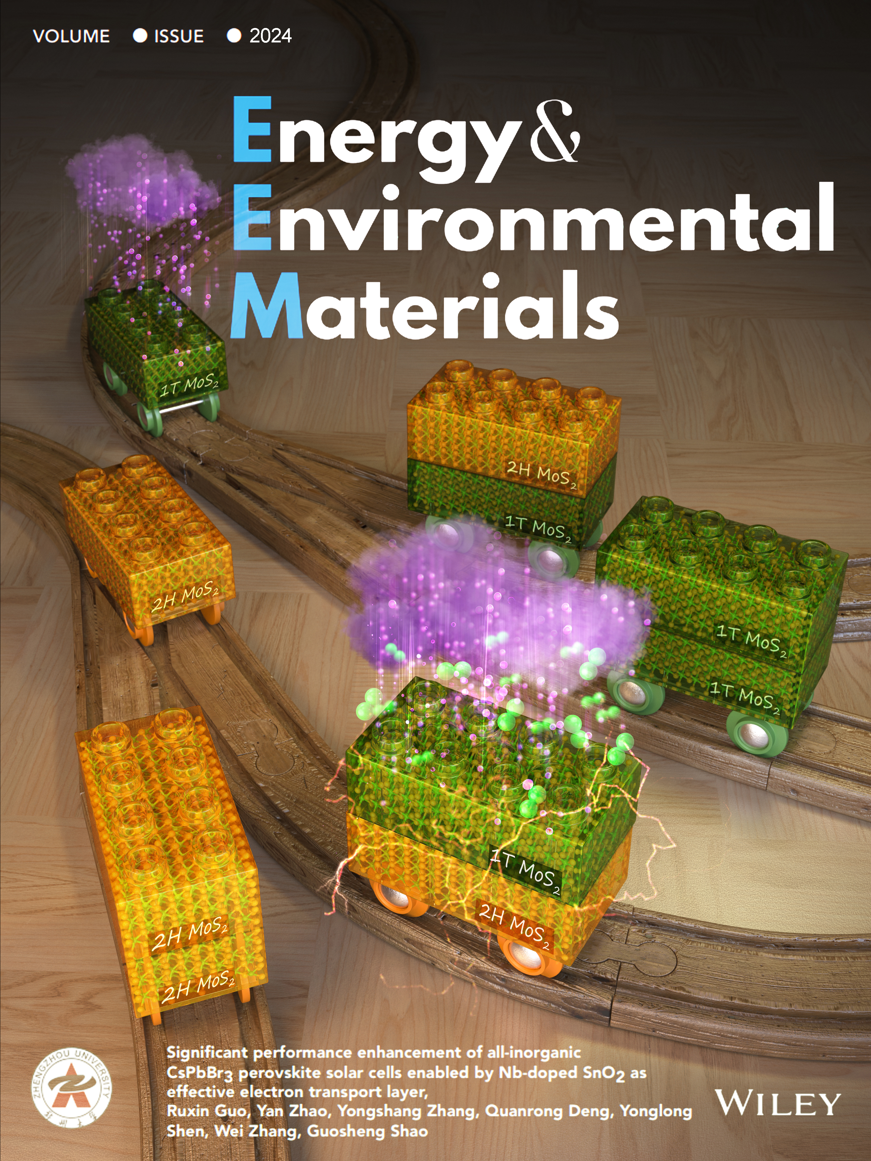
□ KIMM has secured original technology for the two forms of 4-inch heterostructure wafer fabrication through patent registrations in both the United States and South Korea. Additionally, the research is featured as a cover article in prominent journals, Advanced Materials** and Energy & Environmental Materials***.
** Paper Information: 「Electron Release via Internal Polarization Fields for Optimal S-H Bonding States」, Advanced Materials, (https://onlinelibrary.wiley.com/doi/10.1002/adma.202411211)
*** Paper Information: 「Unlocking of Schottky Barrier near the Junction of MoS₂ Heterostructure under Electrochemical Potential」 Energy & Environmental Materials, (https://onlinelibrary.wiley.com/doi/10.1002/eem2.12800)
□ This research was supported by KIMM's core project on plasma equipment-based foundational technology development for semiconductor and display industry processes, KIMM's Creative Challenge Research Program, and the Ministry of Trade, Industry, and Energy's Human Resources Development Project.

Reference Material 1. Plasma synthesis equipment
Reference Material 2. Actual fabricated 4-inch WS₂-Graphene heterostructure sample photo,
and atomic layer cross-sectional TEM image


Reference Material 3. Selected as covers in recognition of research excellence:
Advanced Materials (left) and Energy & Environmental Materials (right).


